Nadca 207 and input material quality control in the tool shop
Even before I deal with the practical possibility of applying this simplified control of steel input quality using Nadca 207 maps for annealed structures (Fig. No. 1) directly in the tool shop, it is necessary to answer a few questions:
– Do I really want to do it?
– Do I have the equipment?
– Do I have the expertise?
– Do I have time for that?
– Do I have the money?
Let’s face it, I would answer all these questions myself – NO. The reason is that the only independent, professional and reliable inspection is the impact tests in an accredited laboratory. They have already figured this out in Škoda-Auto, and although the initial metallographic inspection was previously performed by Professor Horyna from Liberec, today they are already performing the impact tests for all critical parts.
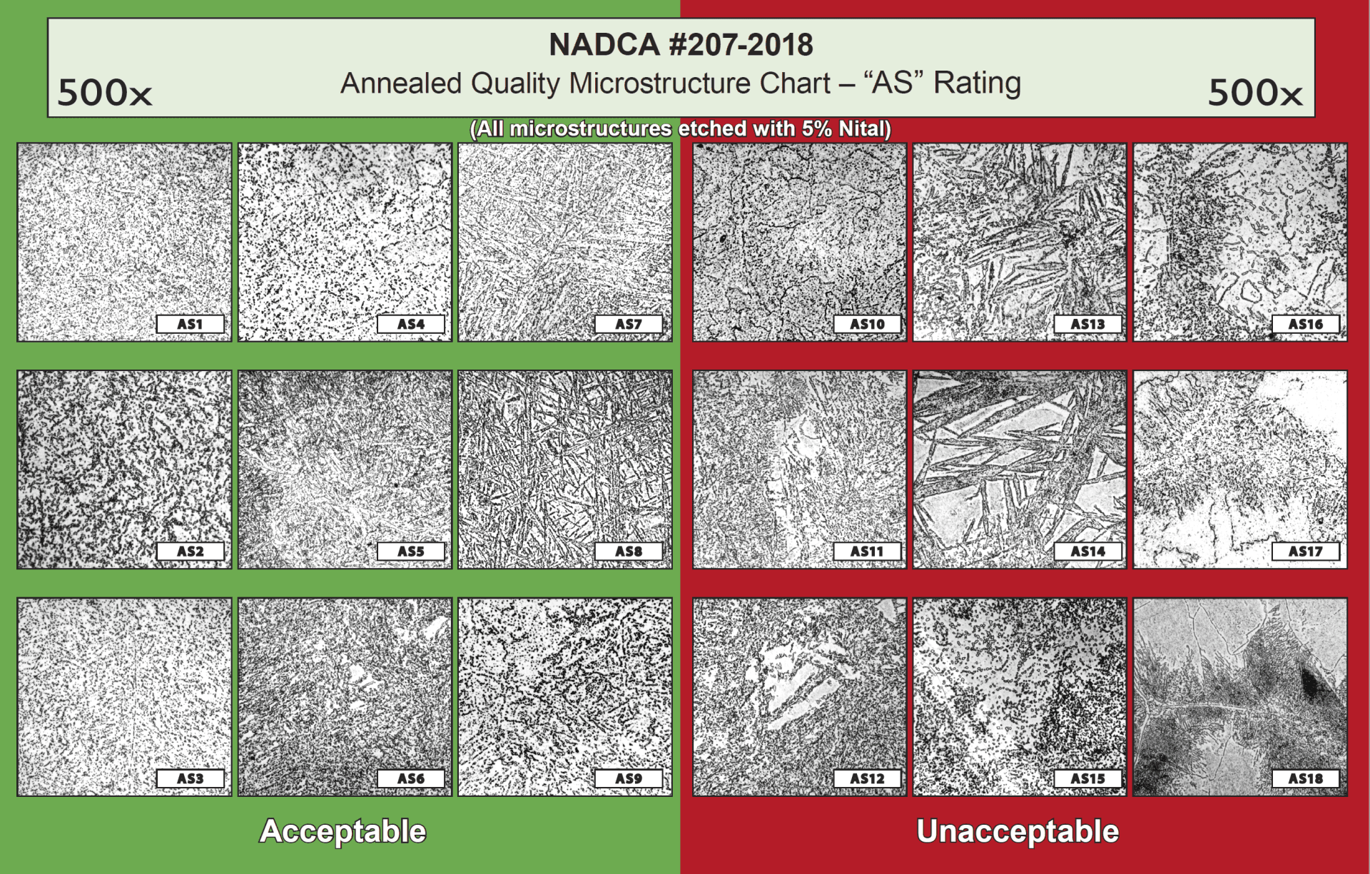
Fig. 1 – Maps of acceptable and unacceptable structures for annealed material
However, in practice there may be cases where we want to use it, but we are not equipped for it and we do not have the expert to do so. Is there a way?
Every tool shop producing die-casting dies should ensure that no white remelted layer is present on the surface after EDM application. If EDM is applied before hardening, it may turn out as in this example (Fig. 2), when the remelted layer was not removed and the stress annealing after EDM was not included.
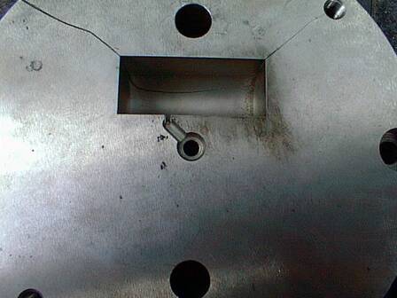
Fig. 2 – Cracks due to incorrectly applied EDM before hardening
If EDM is performed after hardening, then this is fine, but we must be sure that the white remelted layer is removed. Usually by grinding, polishing, blasting. But how to check it? The solution is relatively simple. The white layer is called „white“ because, when etched, the layer appears white under a microscope, with no indication of the material’s own structure. This can be seen in Figure 3 below.
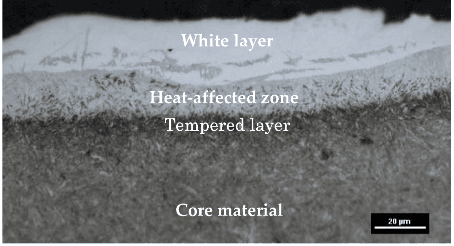
Fig. 3 – Layer structure after EDM (source : Multi-Response Optimization of Electrical Discharge Machining Using the Desirability Function, Rafał Świercz, Dorota Oniszczuk-Świercz, Tomasz Chmielewski, XIII Internation al Conference Electromachining 2018 that was held in Bydgoszcz, Poland, 9–11 May 2018).
Therefore, if we have in workshop portable microscope, preferably with a magnification of up to 500x, after mechanical removal of the layer, we polish the surface where we want to verify the presence of the remelted layer, and etch it with a metallographic etchant called Nital 5%.
Subsequently, we should see either a white, unetched area at the analyzed surface, which is a sign that the layer has not yet been removed, or signs of an etched martensitic structure of the material with possible carbides, indicating that we are already in a zone thermally affected by EDM.
The ideal device for such an inspection is the Keyence VHX 7000 digital microscope mentioned on my blog (Fig. 4). It cannot only magnify up to 6000x, but also capture images in 4K display, with a high depth of field, can be mobile, connected by a cable up to 20 m to a computer unit. However, this microscope can also measure, and therefore it is possible to imagine its use for shape control, accurate measurement of vent channels, etc., it can also perform complete image analysis and other specialties. The only disadvantage is the price, but balanced by high added value. Contact for the supplier is here: Jiří Vaněček, KEYENCE INTERNATIONAL (Belgium) NV / SA, Office Park Kavčí Hory, Na Hřebenech II 1718/10, 140 00 Prague 4, j.vanecek@keyence.eu
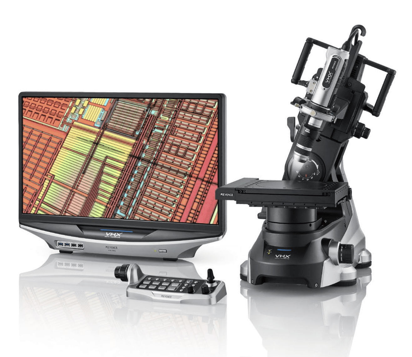
Fig. 4 – Digital microscop Keyence VHX-7000
The opposite of this microscop are simple digital USB microscopes according to Fig. 5. Their price is only 700 to 1000 CZK, which is tempting, but the result is useless. I bought it personally, but one disappointment after another. The problem will start with the SW installation. This is a Chinese product with Chinese SW. Installation on my computer or laptop failed, it does not understand to Win 10 or Win 8. But when I managed to get the camera up and running, the result was unusable at about 100x magnification. The low resolution of the CMOS sensor and the inability to focus the image will prevent its use in practice. The stand and the camera are made of plastic, so the whole device shakes with every touch. Focusing alone is a huge problem.
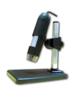
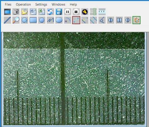
Fig. 5 – ProHard 2.0 digital USB microscope and display of H11 steel structure at a magnification of approx. 500x.
After a long period of investigation and with the help of Mr. Černický from Metalco, I came up with something that could really be used for the given purpose in the conditions of the tool shop, and at the same time it would be for quite reasonable money.
A. Measuring microscope from Befort- Optic
(https://www.befort-optic.com/en/messmikroskope.php)
It is a simple device, basically a metallographic magnifying glass, with various lenses and with illumination (Fig. 6). At the highest magnification of 100x, its resolution is 10 µm. However, we need a magnification of 500x, because in addition to the control of the white layer after EDM, we would also like to perform an input control of steel according to Nadca 207 maps, both for annealed structures and for structures after hardening. This device does not allow us, however, for example for the inspection of polished or patterned surfaces with falling inclusions, scratches, grooves, it is possible to imagine its use in the tool shop
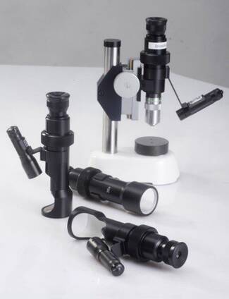
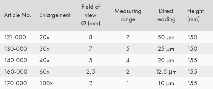
Fig. 6 – Measuring microscope from Befort-Optic with magnification up 100x
B. Portable microscope from OPTO
(https://www.opto.de/en/microscopy/application-microscopes/portable-microscope/)
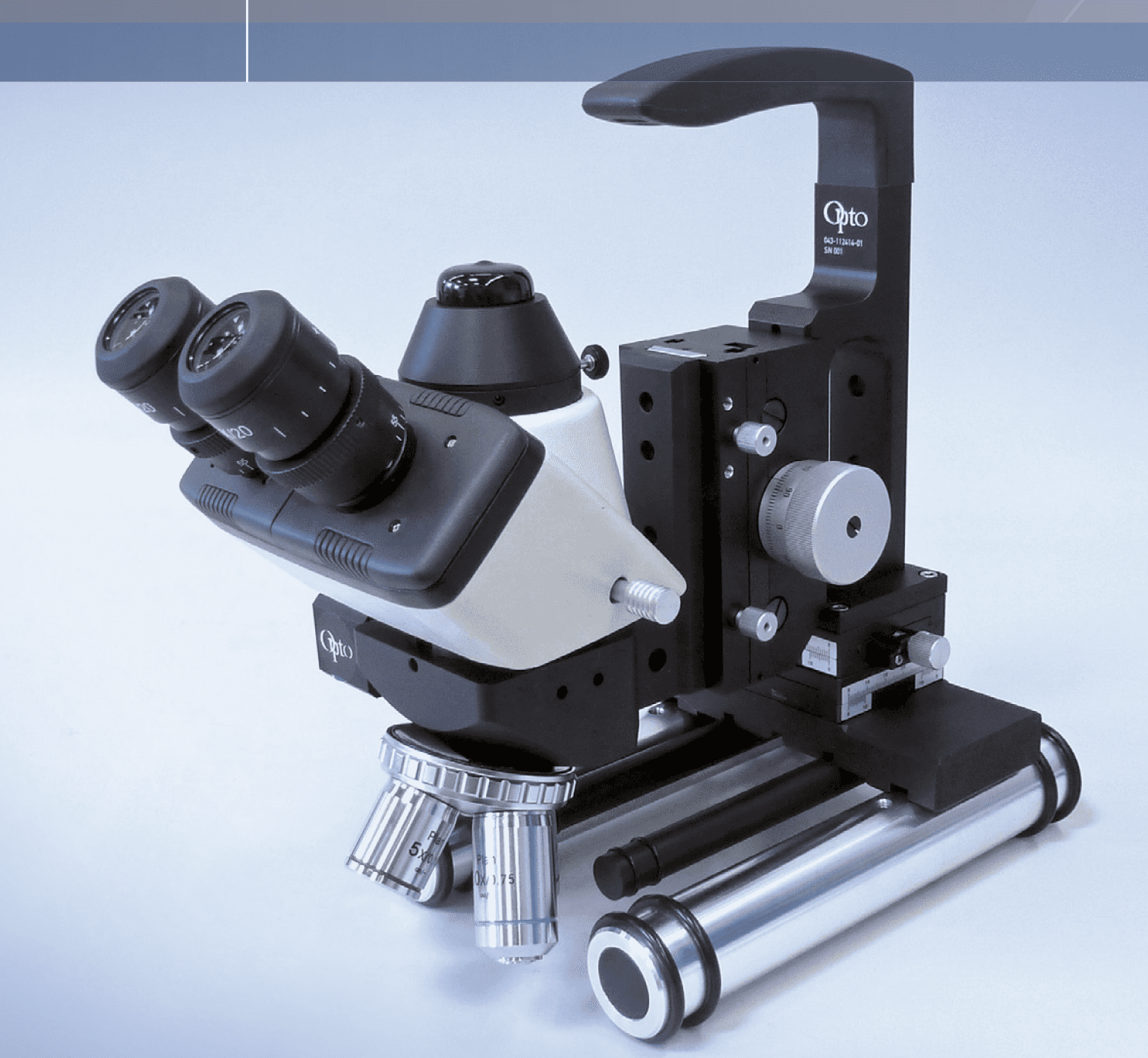
Another solution is a portable microscope from OPTO (Fig. 7). This device is already professional enough and is adapted for field work. It is possible to choose lenses with a magnification of 50x, 100x, 200y and 500x, and it is also possible to place a digital camera on it, directly from the manufacturer or your own, with OPTO or even your own software. Its weight of 5 kg guarantees sufficient stability and resistance to shocks.
Fig. 7 – Portable microscope from OPTO
Even with full hardware and software, we will already be at reasonably priced levels, even if this device is not free either. If you are interested, you can contact Mr. Dipl. Ing. David Černický, Metalco company, E-mail: david.cernicky@metalco.cz
C. Struers PSM 5 and 10
Because the market offer is not very rich, the latest instrument is a portable microscope from Struers (Fig. 8). It is available in PSM 5 or PSM 10 versions. The difference between the models is that PSM 10 allows magnification up to 600x, with PSM 5 only 400x. The device can again be equipped with a digital camera with a CMOS sensor and a 10 “display. Because we need a record of the performed inspection for the needs of the delivery of the die, in all cases I consider the digitally scanned image and its archiving to be a condition for the successful use of this self-inspection, even in for possible future disputes.
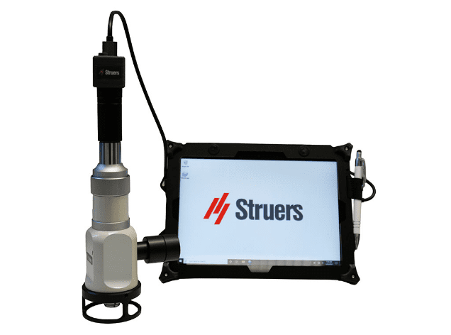
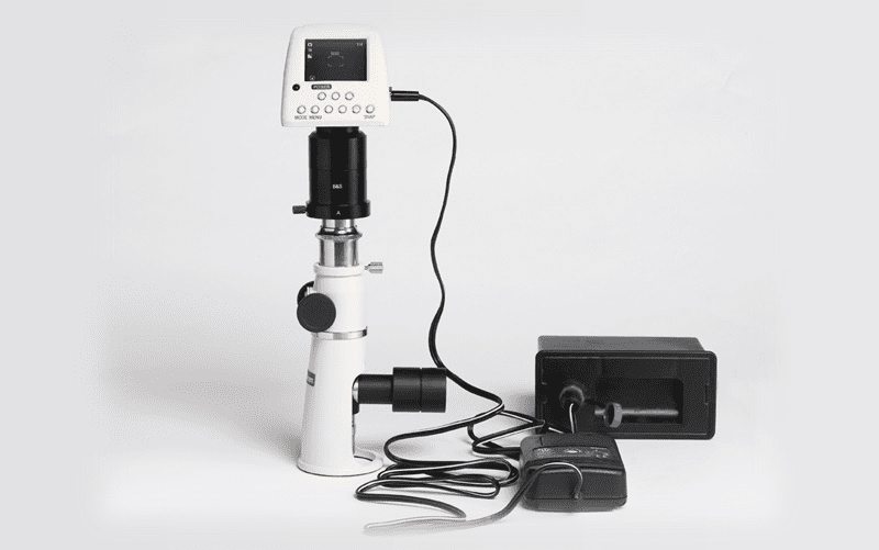
Fig. 8 – Portable microscope Struers
Because we need to grind and polish the measuring spot on the surface, both for the analysis of the removal of the remelted layer after EDM and for the control of the annealed structure of the input material, which we then etch with NITAL 5% etchant, we need both this etchant and polishing equipment.
There is no problem with the Nital 5% etchant, it can usually be purchased from suppliers of consumables for metallography (Fig. 9).
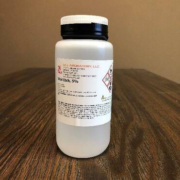
Obr. č. 9 – Example of NITAL 5%
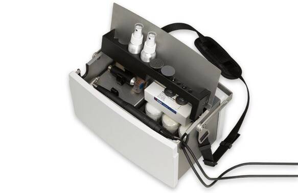
Obr. č. 10 – TransPol 5 set for grinding and polishing from Struers
With the preparation of the surface for measurement, ie grinding and polishing the surface, it is a bit more complicated. It is possible to choose a professional solution such as the TransPol 5 grinding and polishing equipment from the Struers company (Fig. 10), or in every tool shop for manual finishing operations there is always a person who knows this and has the equipment for it.
I can imagine this “autonomous” solution when controlling the remelted layer. However, if we are also engaged in regular incoming inspection of the material, then the incoming inspection must have complete equipment, independent of the manual operations of the tool shop.
However, it is also possible to think about electropolishing with the MoviPol5 device (Fig. 11), again from the Struers company, which can combine both necessary operations, ie polish the measured area and then etch it, within 1 minute.
Both the TransPol 5 and MoviPol 5 polishing machines are battery-operated and fully portable, so they can be used anywhere in the tool shop hall.
For your own microscope, it is probably appropriate to purchase a magnetically clamped holder (Fig. 12), which fixes the microscope and eliminates any problems with vibration of the instrument.
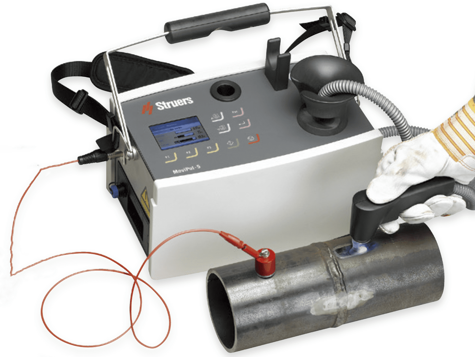
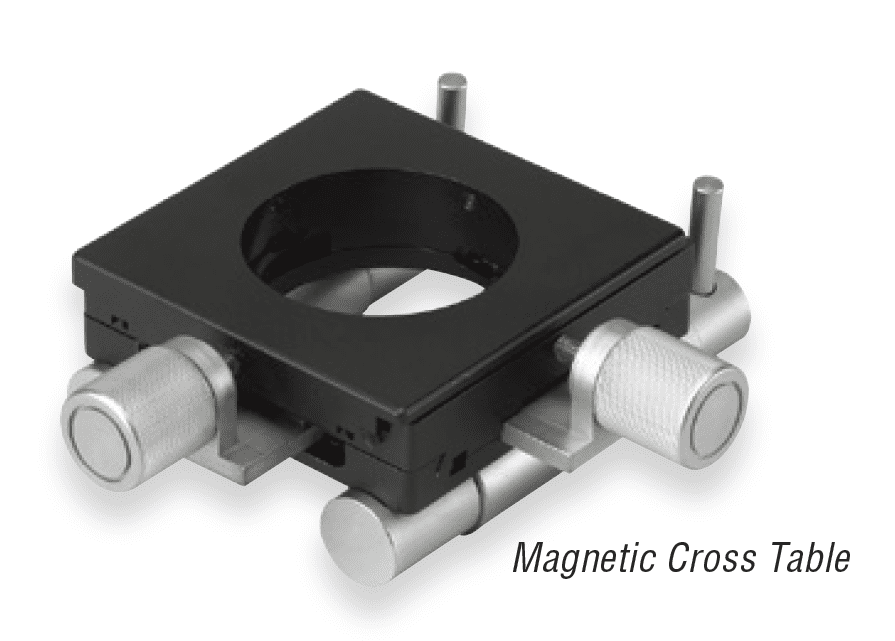
Fig. 11 – MoviPol 5 electropolishing machine from Struers
Fig. 12 – Magnetically clamped microscope holder
Any questions can be raised directly to the Struers representation, to Mr. Ing. Martin Láska, Ph.D., Struers GmbH, Science and Technology Park, Přílepská 1920, 252 63 Roztoky u Prahy, Czech Republic, martin.laska@struers.de
So what is the conclusion? The priority for the tool shop, which produces die-casting dies, is to control the removal of the remelted layer after EDM. The tool maker has to be equipped and qualified to do that. However, if the tool maker is reaching this qualification, then the transition to the initial material control according to the maps of Nadca 207 will no longer be so painful, because we already have the necessary equipment and expert for analyzing the result. .
May 12, 2022
Jiří Stanislav